
Input conditioning is one of those things that snares novice designers, causes late-process changes that overrun expectations on cost and board area, and traditionally isn’t terribly well taught to EE/CPE students.
It’s on my mind because next week is the point in the semester where I drag UK’s current crop of EE/CPE sophomores through a lab exercise I designed about 5 years ago to drive home gate delays, static hazards, switch bounce, etc.
While I was thinking about it, an upperclassman who regularly digs up neat stuff sent me the cleverest input conditioning circuit I’ve ever encountered.
The circuit comes from the late, great Don Lancaster of TV Typewriter fame, who in addition to his published designs, wrote and self-published a number of instructional/reference books. He had a well-deserved reputation for clever, cheap, robust circuit designs, and this particular trick is the highest wizardry.
Here’s the whole circuit diagram from the text:
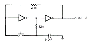
The design comes from his CMOS Cookbook (PDF, link to his own hosted copy of the 2nd ED), on p.317 amid a discussion of Flip-Flops and Clocks. It is presented as “An Alternate-Action Push Button” which is entirely correct but really undersells how clever it is, and has apparently been in there since the 1st edition in 1977.
Here’s a link to it pre-built in the CircuitJS simulator so you can manipulate it and see it work. I had to play with it for a few minutes before I really understood the genius.
The fundamental trick is that it’s a master-slave Flip-Flop where the capacitor is the master storage element, and the pair of feedback-coupled inverters is the slave. The cap tanks the next state based on the output of the first inverter when the switch is open, and induces it on the inverters on switch close. This means, in addition to latching/toggling, it de-bounces, because the capacitor sets the time constant for hysteresis. It conditions, because the load sees the output of the second inverter. No race conditions or potential oscillations, because the cap can’t charge/discharge while the switch is held. No charge is moving inside the mechanism at steady state, so it’s not leaking power. It’s brilliant.
It is only suitable for relatively slow human-scale edges, so probably not a good method for encoders or the like. You can manipulate the time constant for the de-bounce by changing the value of the capacitor, but only down to a few 10s of nF (depending on what kind of inverter you use) before it gets marginal because it doesn’t have the charge to reliably throw the input of the first inverter.
Not only is it ridiculously cheap and simple as presented, which I think intends a 4067 or 74HC04, you can built it out of anything. Any inverting CMOS gate will work. Any inverting TTL gate will work. Ridiculous old RTL or DTL inverters work. A pair of N-Channel FETs (another CircuitJS link, has an extra transistor on the output for integrity reasons) with pullups to build your own cruddy NMOS inverters works. As would P-channels with pull-downs, or BJTs with resistors for constructed RTL (though doing it that way is leaky), or various other assemblages of tiny mass produced minimum cost components to make it even more minimal (though maybe not cheaper in a modern context).
I appreciate a clever domain-crossing design, and this is the highest form.
